1. Introduction
he adder is one of the most critical components of a central processing unit. The object of the adders not only adding of bits but also involves in address calculation, subtraction, division and multiplication, the adders are critical components to determine the speed, delay and power of the overall system, low power adders are always preferable. Due to the popularity of portable electronic products low power system has attracted more attention in recent years, an system on chip (SOC) design can contain more and more components that lead to a higher power density. This makes power dissipation reach the limits of what packaging, cooling or other infrastructure can support, reducing the power consumption not only can enhance battery life but also can avoid the overheating problem which would increase the difficulty of packaging or cooling. Therefore the consideration of power consumption in complex SOCs has become a big challenge to designers, moreover in modern VLSI designs [3][4][5].
Lowering power is one of the greatest challenges facing the IC industry Today, temperature profile and battery life requirements for tethered and un tethered systems have made power consumption a primary optimization target for IC industry [2]. IC power consumption consists of three basics components: switching power, short circuit power and leakage power [6][7].
Dynamic power
2 DD L D V f C 2 1 P = (1)Dynamic power is square of supply voltage, therefore by reducing supply voltage we can reduce dynamic power [8].
The leakage power is mainly due to sub threshold current and it may be defined as the drain to source current of the transistor operating in the weak inversion region of MOSFET this subthreshold leakage may be defined as in eq (2) give s a simple method for estimating the leakage current in a single NMOS transistor [9][10][11].
( )
? ? ? ? ? ? ? ? ? ? ? ? ? ? ? ? ? ? ? ? ? ? = t ds t t gs v V V v V I exp 1 exp I 0 s ? (2)V t is the thermal voltage and is given by Q/KT and n is the sub threshold slope coefficient. Generally there are varies leakage reduction techniques based on mode of operation of systems the two operation modes are active mode and stand by mode or idle mode. Most of the leakage power reduction techniques will be based on idle mode [12]. SECTION2: gives an overview of the Novel PMOS and NMOS and their simulation results, SECTION3 presents Novel 3 bit full adder and conventional full adder, SECTION 4 describes experimental results of conventional, Novel full adders and DTMOS full adders, SECTION5gives conclusions.
II.
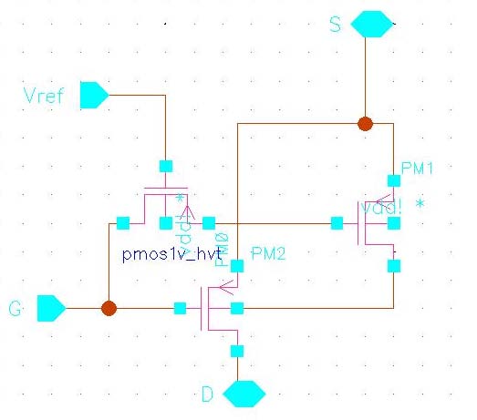
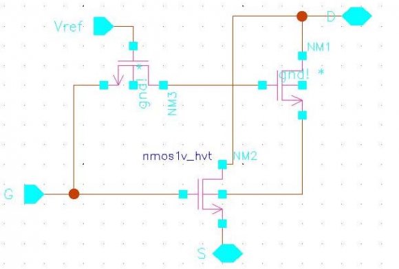
2. An Over View of Novel PMOS and NMOS
Ultra low power operation plays a major role in designing of CMOS circuits in subthreshold regime, for any digital or analog design the basic components are PMOS and NMOS devices, the power consumption of this basic elements determine the overall power of the system. In this section we provide Novel PMOS and NMOS, simulations have been carried out in cadence design frame work to verify the functionality of the
3. A Conventional CMOS Adder
The 28 transistor full adder is the pioneer traditional adder circuit, the schematic of this adder is shown. This adder cell is built using equal number of NFET and PFET transistors, the MOS logic can be realized using equations [1].
Carry: AB+BC+AC (2) SUM: ABC+(A+B+C)C(3)The conventional full adder consumes more power compared to Novel full adder, both conventional and Novel full adders are simulated and their average power is calculated [14].
4. Simulation Results and Analysis
An investigation has been carried out for calculating average power, static power of conventional full adder and the Novel full adder and compared their powers at 45nm technology using virtuoso design environment.
A novel CMOS adder may have an overhead area, but it consumes less power [15].
5. Conclusions
The performance of many large circuits are strongly dependent on the performance of the full adder circuits that have been used. An attempt has been made to design 84T novel full adder with low power consumption. In this paper we have simulated conventional full adder and Novel full adder and calculated average power. As mentioned earlier as the technology advances apart of dynamic power, there will be a equal part of leakage power, therefore a Novel full adder will suitable for low power design.

| Voltage Is 0.6v | |||
| Parameter | Full Adder With Novel PMOS & NMOS | Conventional CMOS full adder | DTCMOS full adder |
| Avg. Power | 97.23nw | 105.8nw | 243nw |
| Delay | 150ps | 580ps | 291ps |
| PDP | 1.456×10⁻¹⁷ | 61×10-15 7.07×10⁻¹⁷ | |
| Conventional CMOS Full Adder Versus Novel Full Adder | ||
| at 45nm and Supply Voltage Is 1.1v | ||
| Parameter | Full Adder With Novel PMOS & NMOS | Conventional CMOS full adder |
| Avg. power | 0.43µw | 1.88µw |
| Delay | 72ps | 43ps |
| PDP | 3.152×10 -17 | 8.084×10 -17 |
| Adder and Conventional Full Adder with Supply Voltage | ||
| of 1.1v @180nm | ||
| Parameter | Full Adder With Novel PMOS & NMOS | Conventional CMOS full adder |
| Avg. power | 69.49µw | 32.8µw |
| Delay | 217ps | 166ps |
| PDP | 15×10 15 | 5.45×10 15 |
| Adder, DTCMOS Full Adder and Conventional Full | |||
| Adder at 45nm with 0.6v | |||
| Parameter | Full Adder With Novel PMOS & NMOS | Conventional CMOS full adder | DTCMOS full adder |
| Static power | |||
| when all inputs are at | 9.159pw | 8.688pw | 109.4nw |
| 0.6v | |||
| Static power | |||
| when all inputs are at | 14pw | 8.756pw | 78nw |
| 0v | |||
| Adder and Conventional Full Adder at 45nm With1.1v | ||
| Parameter | Full Adder With Novel PMOS & NMOS | Conventional CMOS full adder |
| Static power when | ||
| all inputs are at | 44.6pw | 30.97pw |
| 0.6v | ||
| Static power when all inputs are at 0v | 52.18pw | 28.76pw |
| Adder, And Conventional Full Adder At 180nm With1.8v | ||
| Parameter | Full Adder With Novel PMOS & NMOS | Conventional CMOS full adder |
| Static power when | ||
| all inputs are at | 30.97pw | 69.25pw |
| 1.8v | ||
| Static power when all inputs are at 0v | 590pw | 97.5pw |
| V. | ||