1.
hree-level inverters have attracted the attention of researchers since their introduction by Nabae et at. [1] in 1981. Though simple and elegant, neutral-clamped circuit topology has a few disadvantages. Neutral point fluctuation is commonly encountered as the capacitors connected to DC-bus carry load currents. Also, there is ambiguity regarding the voltage rating of the semiconductor devices, which are connected to the neutral point. This calls for a conservative selection of devices for reliable operation, which, however, increases cost. Various alternative circuit topologies have been suggested in the literature. H-bridge topology [2], [3] eliminates the problem of neutral fluctuation, but requires three isolated power supplies. Soh and Hyun [4] have suggested an improvisation of the conventional neutral clamped inverter in which a capacitor is connected across the neutral clamping diodes to ensure dynamic balancing of the voltage across the DC bus capacitors. This method alleviates the problem but does not eliminate it. Three-level inversion may also be achieved with two 2level inverters, driving an open-end winding induction motor from either end [5], [6]. The inverters in this case require isolated power supplies to eliminate the harmonic currents of the triplen order in the individual motor phases Recently, Somasekhare t al. [7] have suggested an open-end winding induction motor drive, which obviates transformer isolation. But the DC bus utilization is slightly lower in this scheme when compared to the schemes proposed by Stemmler and Guggenbach [5] and Shivkumar et al. [6] The DC link capacitors in this circuit do not carry the load currents and hence the voltage fluctuations in the neutral point are absent. Also, the circuit configuration needs two isolated power supplies compared to H-bridge topology, which requires three isolated power supplies to achieve 3-level inversion. However, the power semiconductor switches in one bank (three in number) in one of the inverters of this circuit have to be rated for the full DC link voltage. ? corresponding leg in Inverter2 is turned on. In this case, the DC input point of that phase for Inverter2 is floating as the top and bottom switches are switched complementarily in any leg in a 2-level inverter. This means that individual inverters are operated with a DC link voltage of 150 V. The motor is run in open loop using the V If control scheme. To demonstrate the working principle of this inverter scheme, space vector, modulation has been employed, which was implemented using look-up table approach. The space vector combinations at each space vector location have been chosen in such a way that both the inverters are switched with only one transition during the subinterval period.
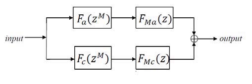
A three-level inverter configuration with common mode voltage elimination is already presented in [10]. Only those switching combinations, which generate zero common mode voltage in the inverter poles, are used to switch the three-level inverters from both sides, thus resulting in zero common mode voltage across the machine phases [10]. Thus, appropriate selection of switching states, of individual three-level inverters, result into the total elimination of alternating common mode voltage from the inverter pole voltages as well as common mode voltages from the phase windings of the induction motor [10]. As the common modes voltages are absent in this scheme, individual three-level inverter structure can be supplied from single dc link as shown in Fig. 1. The three-level structure is realized by cascading two conventional twolevel inverters, resulting in a simple power bus structure for the proposed power circuit [9], [10]. The unbalance in the dc link capacitor voltages for the proposed openend winding induction motor drive.
As explained in the previous section, the inverter space vector locations have multiple switching combinations of inverter-1 and inverter-2 voltage space vectors (Fig. 2). The central voltage location being referred as zero voltage vector (ZV), the voltage vector locations at the periphery of inner hexagon are referred as small voltage vectors (SV), the intermediate voltage vectors on outer periphery are referred as middle voltage vectors (MV), while the largest voltage vectors on outer periphery are referred as large voltage vectors (LV). a) Back-to-Back Intertie When interconnecting two diode-clamped multilevel inverter to-gather with a "dc capacitor link," as shown in Fig. 2 the left-hand side converter serves as the rectifier for utility interface, and right-hand side converter serves as the inverter to supply the ac load. Each switch remains switching once per fundamental cycle. The result is a well-balanced voltage across each capacitor while maintaining the staircase voltage wave, because the unbalance voltages across each other tend to compensate each other. Such a dc capacitor link is categorized as the "back-to-back intertie." The purpose of the back-to-back intartie is to connect two asynchronous systems. It can be treated as 1) a frequency changer, 2) a phase shifter, or 3) a power flow controller. The power flow between the two systems can be controlled bidirectionally. An ideal utility compatible system requires unity power factor, negligible harmonics, no EMI, and high efficiency. By extending the application of the back-toback intertie, the multilevel inverter can be used for a utility compatible adjustable speed drive (ASD) with the input from the utility constant frequency ac source and the output to the variable frequency ac load. The major differences, when using the same structure for ASD's and for back-to-back intertie, is the control design and size of capacitor. Because the ASD need to operate at different frequencies, the dc link capacitor needs to be well-sized to avoid a large voltage swing under dynamic condition.
2. c) Converter Topology
Rectifier Operation Inverter Operation DC Link
3. Table2 : Output voltages and capacitor currents
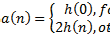
Where 'n' is the order of the harmonic and 'w' is the angular frequency. The voltage levels of the dc sources are equal and labeled to be V dc . Also, the voltage of the capacitors is same and intended to be regulated at the modulation index in general is defined as:
Modulation Index M: V m /V dc Where, Vm is the magnitude of the fundamental component of the output voltage.
4. Theta Calculations
Considering only the fundamental component and eliminating the 3rd and the 5th order harmonics, the following equations are used to calculate 1, 2, and 3 for different values of the modulation index 'M'.
Here 'p' is considered to be three.
5. 2012
April from USV or LSV groups can be selected for inverter switching, which will bring back the deviation in the capacitor voltages to zero. This is done using a hysteresis controller. The input to the controller is the difference between the dc link capacitor voltages; the normal control band is set depending upon the maximum deviation that can be allowed in the dc link voltages. The controller outputs, 0 if the is within the ab ca nt normal band, 1 if is greater than the control band and 1 if the is less than the control band. The schematic of the closed loop voltage balancing scheme is shown in Fig. 5. The output of the controller along with "SEQ" signal is used to select the appropriate value of the signal "state," which is given to a digital logic.
6. Fig5 : Hysteresis Controller Based Closed Loop DC Link Balancing Scheme
It is to be noted that only the inverter vectors belonging to USV or LSV groups have strong capability to charge/discharge the dc link capacitors. During motor operation in over-modulation range, the inverter vectors belonging to MV and LV groups are switched for maximum duration, in a switching interval, as compared to the inverter voltage vectors belonging to SV group. The extreme case is the 12-step operation, wherein the inverter vectors from the SV group are not switched at all. Under steady state and dynamic operation, in overmodulation, the controller can maintain the capacitor voltage balance by switching MV and LV vectors. The SV vectors are switched for less time duration, the time required to bring back the capacitor voltages to the balanced state, is more during over modulation operation. In extreme case, the inverter vectors from SV group are not switched in 12-step mode. If there is mismatch in the capacitor voltages due to the asynchronous PWM or asymmetric loads, the capacitor voltages are balanced by reducing the modulation index momentarily. This allows the switching of the inverter vectors belonging to SV group and the dc link capacitor voltages are brought back to the balanced state as shown in the simulation results of Fig. 6. Thus while, USV vectors were having charging effect on C1 and discharging effect on C2 in motoring mode, they have discharging effect on C1 and charging effect on C2 in regenerative mode. Thus, the controllers need to sense the power direction, to suitably switch the switching combinations belonging to the vector group, which will reduce the error in the dc link capacitor voltages.
Determining the operating mode (i.e., motoring/generating) requires current sensing. The determination of current direction for currents drawn from dc link involves hardware sensors or can be judged from direction of power flow Fig. 6 : DC link balancing with momentary reduction in modulation index.
If the motor is operating in regenerative mode, the actions taken by the controller will worsen the voltage balance. An additional hysteresis comparator is used to sense this change. The control band of this comparator is placed above the control band of the main inner comparators. Thus, with motor operating in regenerative mode, the outer comparators of hysteresis controller gets activated if the dc link voltage unbalance exceeds the outer comparator settings and the switching combinations belonging to the USV or LSV vector group, which reduces the voltage unbalance, are selected for inverter switching. As shown in simulation results of Fig. 6, the motor is initially operating in motoring mode and the load torque is made negative thus driving the motor in regenerative mode. The voltage balancing controller is disabled which will cause rapid growth in dc link unbalance. When the voltagebalancing scheme is enabled again, the capacitor voltages are brought back to the normal value, similar to the case with motor operating in motoring mode. The three-level structure is realized by cascading the conventional two two-level inverters, resulting into simple power bus structure for the proposed scheme. Thus, the proposed inverter structure does not require any clamping diodes which are required in NPC inverter topology. The proposed scheme has more multiplicity in the inverter voltage vector locations as compared to conventional single inverter fed drive which are effectively used to balance the dc link capacitor voltages without disturbing the SVPWM modulation. Thus, a single front-end rectifier of rating nearly half to that of a conventional two-level inverter can be used, with two capacitors for splitting the dc link voltage The performance of these methods is studied through Matlab simulation.. It is clear that there is a reduction in THD. Next aspect that was looked into was the effect of power factor on output voltage and load current.
7. Global Journal of Researches in Engineering