1. I. INTRODUCTION
roup III-V nitride are now a widely studied class of semiconductor materials. In x Ga (1-x) N, with small x, are very ef ficient light emitters, even in samples with relatively high densities of structural defects are used as component layers in a wide range of optoelectronic devices. Its high light absorption and its Indium-composition-tuned band gap, the Indium Gallium Nitride (InGaN) ternary alloy is a good candidate for high-efficiency-high-reliability solar cells able to operate in harsh environments.
Moreover, the most important advantage of InGaN alloy might be the direct band gap energy which can be adjusted according to the indium composition.
Thus, the InGaN's energy band gap can be tuned from 0.7 eV to 3.42 eV, covering approximately the total solar spectrum [1]. In this paper, we present simulation of InGaN based p-n homo junction solar cell at different Indium composition . The layers of InGaN solar cell can be deposited using the cost-effective techniques, such as Metal Organic Chemical Vapor Deposition (MOCVD), Metal Organic Vapor Phase Epitaxy (MOVPE), and Molecular Beam Epitaxy (MBE) [2]. Whatever the deposition technique used, higher growth rates (~1.0 Angstrom/second) and lower temperature(~550 °C) characterize the InGaN growth
2. (
)
InN GaN g x g g 1-x In Ga N =x.E +(1-x).E -b.x.(1-x) E (1)where the band gap energy of InN denoted as ?? ð??"ð??" ?????? and band gap energy of GaN denoted as ?? ð??"ð??" ?????? is 0.7eV and 3.42eV, respectively, x is the indium content and ?? is the bowing parameter (?? = 1.43) [5][6].
The other modeling parameters of the In??Ga (1-??)N alloy were calculated using the following equations-Electron Affinity [7][8][9]: -
( ) ( ) 1 4.1 0.7(3.4 ) x g x In Ga N E ? ? = + ? (2)Relative permittivity[6]: -
( ) ( )115.3 8.9(1 ) ( ) 18 1 (0.9 2.3(1 )).10
x x In Ga N x x ? ? = + ? (3)C x x N In Ga N x x ? = + ? (4)Effective density of valence band [8][9]: -
( ) ( )19 1(5.3 1.8(1 )).10
V x x N In Ga N x x ? = + ? (5)3. b) Physical & Optical Perameters
The energy band gap of In x Ga (1-x) N is depended on concentration of Indium (x) and energy band gap of In x Ga (1-x) N is given by following formula ( )
(GaN) 1 (524* x) n x n x U In Ga N U ? = +(11) ( ) ( )h(GaN) 1 (6.5* x) h x x U In Ga N U ? = +(12)Where the U n(GaN) is 1000 & U h(GaN) is 170.
For the In??Ga 1-?? N alloys, Adachi's wavelengthdependent refractive index model is given by the following equation [6,12]:
2 E E E (E) 2 1 1 B E E E ph ph ph g g g n A ? = ? + ? ? + ? ? ? ? ? ? ? ? ? ? ? ? ? ? ? ? .......(13)Where Eph is photon Energy A & B is coefficient dependent on material composition that equation giving by following equation. This real part of refractive index is approximate same 2.32 Its slightly worry for InGaN alloy with different composition of x from 2.30 to 2.34.
The InGaN alloys absorption coefficient ?? is given by equation ( 16) [13] ( )
4. (
) Mobility [11]: -
5 2 1 10 (E E ) D(E E ) x ph g ph g x In Ga N C ? ? = ? + ? ???????????????????(B B i i B U U T U N T U ? ? ? ? = + ? ? ? ? + ????????????????????(10)( ) . . % SC OC in I V FF P ? =(9)Where I SC is short circuit current, V OC is open circuit voltage, P in is incident optical power and FF is fill factor of the solar cell. [10] ( ) ( ) 1 0.17 1.0(1 ) Intrinsic carrier concentration: -
h x x m In Ga N x x ? = + ? (7)2 g B E K T i C V N N e n ? =(8)Where K B is Boltzmann constant and T is lattice temperature Efficiency: -
Velocity of electron & hole (S n,h ) [cm/s] 10 35. Recombination time of electron & hole (? n,h )[sec.] 1ns
For the case studied, the initial physical and geometrical parameter values used for In x Ga (1-x) N single p-n junction solar cell are presented in table 6. After modeling & simulation get results with the help of above work following results are tabulates ( )
5 1 1.24 2.2*10 E x g x In Ga N ? ? ? = ? ????.(19)Where ? is photon wavelength
For the In??Ga 1-?? N alloys, wavelength-dependent imaginary part of refractive index is given by the following equation
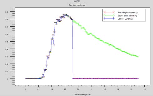
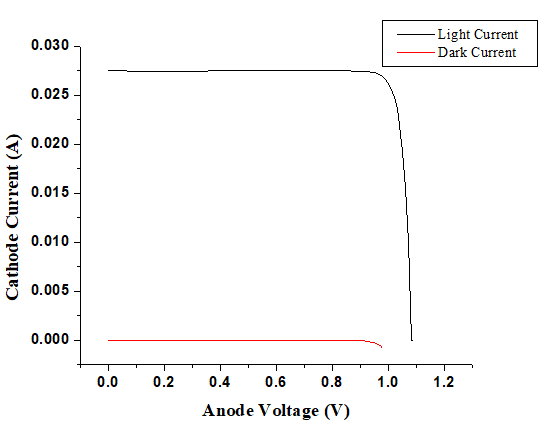
4 K ?? = ? ??????????????(20)Where pie (?) is 3.14. Following Fig. 2 Spectral response with respect to wavelength has been shown above in Fig. 5. Source photo current is maximum possible total current due to incident photons, available photo current is current due to total generated electron-hole pair and cathode current is total current collected at terminals. Among these three, source current is always greater than other two. Total photons incident losses due to reflection, transmission, thermalization etc. Further there is loss of some of the generated electron-hole pairs due to recombination and hence collected cathode current is less than or equal available photo current. After getting all results we gets maximum efficiency is 19.36% at In 0.50 Ga 0.50 N single p-n junction solar cell. This above table 9 shows simulation results of fill factor and efficiency at different composition of x for single p-n junction solar cell. In this paper we report the TCAD simulation and performance optimization of In x Ga (1-x) N based solar cell. Evaluation of the performance of the device has been performed for various values of mole fraction x of In in InGaN. Extracted performance parameters such as current, voltage, power, fill factor and efficiency from the proposed structure are: open circuit voltage (V oc ) of 1.08 V, Short circuit current (I sc ) is 0.027A, Fill Factor (FF) is 88.58%, Maximum voltage (V max ) is 0.99 V, Maximum current (I max ) is 0.26A and overall efficiency is 19.36%. IV.
6. Conclusion
![[3] II. MODELLING AND SIMULATION a) Structure As the numerical simulation is an important way to explore the possibility of a new solar cell structure the InGaN single p-n junction solar cell has been studied using commercial device simulator Atlas from Dilvaco Inc [4].All the simulations were performed under normalized conditions that are 1 sun, a temperature of 300 K, and AM0 illumination. The In x Ga (1-x) N single p-n junction solar cell structure studied consists of p-type emitter and n-type base as shown in Fig.1.](https://engineeringresearch.org/index.php/GJRE/article/download/1956/version/101032/3-TCAD-Based-Simulation-and-Performance_html/22540/image-2.png)
| of electron affinity and relative permittivity | ||
| of In x Ga (1-x) N at different value of x | ||
| Material | Electron | Relative |
| In x Ga (1-x) N | Affinity(X) | permittivity(E) |
| GaN | 4.092 | 8.9 |
| In 0.20 Ga 0.80 N | 4.3955 | 10.18 |
| In 0.35 Ga 0.65 N | 4.5931 | 11.14 |
| In 0.50 Ga 0.50 N | 4.765 | 12.1 |
| In 0.62 Ga 0.38 N | 4.884 | 12.868 |
| In 0.78 Ga 0.22 N | 5.017 | 13.892 |
| In 0.90 Ga 0.10 N | 5.0975 | 14.66 |
| InN | 5.152 | 15.3 |
| Energy Band Gap of In x Ga (1-x) N at x | ||
| Material In x Ga (1-x) N | Energy band gap (Eg) | |
| GaN | 3.42 | |
| In 0.20 Ga 0.80 N | 2.6612 | |
| In 0.35 Ga 0.65 N | 2.1672 | |
| In 0.50 Ga 0.50 N | 1.7375 | |
| In 0.62 Ga 0.38 N | 1.4401 | |
| In 0.78 Ga 0.22 N | 1.1076 | |
| In 0.90 Ga 0.10 N | 0.9063 | |
| Year 2019 | InN | 0.77 |
| 18 | ||
| of Researches in Engineering ( ) Volume XIX Issue IV Version I F | ||
| Global Journal | ||
| © 2019 Global Journals | ||
| Effective density | Effective density | |
| Material | of Conduction | of Valance |
| In x Ga (1-x) N | band (Nc) | Band(Nv) |
| (1×10 18 ) | (1×10 20 ) | |
| GaN | 0 | 0 |
| In 0.20 Ga 0.80 N | 1.8 | 1.06 |
| In 0.35 Ga 0.65 N | 3.15 | 1.855 |
| In 0.50 Ga 0.50 N | 4.5 | 2.65 |
| In 0.62 Ga 0.38 N | 5.58 | 3.286 |
| In 0.78 Ga 0.22 N | 7.02 | 4.134 |
| In 0.90 Ga 0.10 N | 8.1 | 4.77 |
| InN | 9 | 5.3 |
| Effective mass of electron[7] | ||
| Material In x Ga (1-x) N | Mobility of Electron (MUN or Un) | Mobility of Hole (MUP or Uh) |
| GaN | 1000 | 170 |
| In 0.20 Ga 0.80 N | 1104.8 | 171.3 |
| In 0.35 Ga 0.65 N | 1183.4 | 172.275 |
| In 0.50 Ga 0.50 N | 1262 | 173.25 |
| In 0.62 Ga 0.38 N | 1324.9 | 174.03 |
| In 0.78 Ga 0.22 N | 1408.7 | 175.07 |
| In 0.90 Ga 0.10 N | 1471.6 | 175.85 |
| InN | 1524 | 176.5 |
| Material | Effective Mass of | Effective Mass |
| In x Ga (1-x) N | Electron (Mn) | of Hole (Mh) |
| GaN | 0.2 | 1 |
| In 0.20 Ga 0.80 N | 0.184 | 0.834 |
| In 0.35 Ga 0.65 N | 0.172 | 0.7095 |
| In 0.50 Ga 0.50 N | 0.16 | 0.585 |
| In 0.62 Ga 0.38 N | 0.1504 | 0.4854 |
| In 0.78 Ga 0.22 N | 0.1376 | 0.3526 |
| In 0.90 Ga 0.10 N | 0.128 | 0.253 |
| InN | 0.12 | 0.17 |
| Material In x Ga (1-x) N | Isc (mA/cm^2) | Voc (V) |
| In 0.20 Ga 0.80 N | 0.00813315 | 1.9963 |
| In 0.35 Ga 0.65 N | 0.0158621 | 1.51555 |
| In 0.50 Ga 0.50 N | 0.0274789 | 1.08184 |
| In 0.62 Ga 0.38 N | 0.0385468 | 0.781803 |
| In 0.78 Ga 0.22 N | 0.0539032 | 0.446001 |
| In 0.90 Ga 0.10 N | 0.0654447 | 0.242227 |
| ( ) 1 x D In Ga N ( x ? | ) | 0.665 3.616 2.460 x = ? + ? | x | 2 | ?(18) | |||||||||
| Following equation is simplified expression of | ||||||||||||||
| absorption coefficient ?? (19) | ||||||||||||||
| Imaginary Part of Refractive | Index(K) | 0 2000 4000 6000 8000 10000 12000 | x=0.1 | x=0.9 x=0.62 x=0.35 x=0.2 x=0.5 x=0.78 | ||||||||||
| 0 | 0.2 | 0.4 | 0.6 | 0.8 | 1 | 1.2 | 1.4 | 1.6 | 1.8 | |||||
| Wavelength(?) | ||||||||||||||
| Fig. 2: Graph of wavelength vs imaginary part of refrective index at different value of x | ||||||||||||||
| Some initial parameter are given in the following table-6 | ||||||||||||||
| Parameter Used | Value | |||||||||||||
| Thickness of n-InGaN layer | 0.015 micron | |||||||||||||
| Thickness of p-InGaN layer | 0.63 micron | |||||||||||||
| n-type doping [cm -3 ] | 2e18 | |||||||||||||
| TCAD Based Simulation and Performance Optimization of In x ga (1-X) N Based Solar Cell | |||||||||||||
| ( ) 1 x C In Ga N ( x ? | ) | 3.525 18.29 40.22 x = ? + | x | 2 | ? | 37.52 | x | 3 | + | 12.77 | x | 4 | ????????????????????(17) |
| III. RESULT & DISCUSSION | |||||||||||||
| Material In x Ga (1-x) N | Im (mA/cm^2) | Vm (V) |
| In 0.20 Ga 0.80 N | 0.00798644 | 1.88 |
| In 0.35 Ga 0.65 N | 0.01556 | 1.41 |
| In 0.50 Ga 0.50 N | 0.0265989 | 0.99 |
| In 0.62 Ga 0.38 N | 0.0372977 | 0.69 |
| In 0.78 Ga 0.22 N | 0.0507992 | 0.369998 |
| In 0.90 Ga 0.10 N | 0.0563837 | 0.19 |
| Material In x Ga (1-x) N | Fill Factor | Efficiency |
| In 0.20 Ga 0.80 N | 92.4754 | 11.0401 |
| In 0.35 Ga 0.65 N | 91.2636 | 16.1321 |
| In 0.50 Ga 0.50 N | 88.5801 | 19.3624 |
| In 0.62 Ga 0.38 N | 85.3975 | 18.9231 |
| In 0.78 Ga 0.22 N | 78.1818 | 13.8203 |
| In 0.90 Ga 0.10 N | 67.5787 | 7.87713 |
| Year 2019 | ||||
| 22 | ||||
| of Researches in Engineering ( ) Volume XIX Issue IV Version I F | Efficiency | Corporation, International Journal of Photoenergy, Volume 2015, Article ID 594858, 9 pages 2. N. Akter, "Design and simulation of Indium Gallium Nitridemultijunction tandem solar cells," International Journal of Research in Engineering and Technology, vol. 3, no.1,pp. 315 321, 2014. 3. D. V. P. McLaughlin and J. M. Pearce, "Progress in indium gallium nitride materials for solar photovoltaic energy conversion," Metallurgical and Materials Transactions A: Physical Metallurgy and Materials Science,vol.44,no.4,pp.1947-1954,2013. References références referencias 1. Mesrane, F. Rahmoune, A. Mahrane and and A. Oulebsir " Design and Simulation of InGaNp-n Junction Solar Cell" Hindawi Publishing | ||
| Global Journal | 5. F. Bouzid and S. Ben Machiche, "Potentials of InxGa1-xN photovoltaic tandems," Revue des | |||
| Energies | Renouvelables, | vol.14,no.1,pp.47- | ||
| 56,2011. | ||||
| (b) | 6. Z. Li,H.Xiao, X. Wang et al., "T heoreticalsimulations | |||
| Fig. 7: | of InGaN/Si mechanically stacked two-junction solar cell," Physica B: Condensed Matter, vol. 414, pp. | |||
| 110-114, 2013. | ||||