1. I. Introduction
n recent years, the volume of a new developed electronic device has reduced by more than three orders of magnitude compared with several years ago. Thus, it is very important to research an efficient electronic packaging form to improve the efficiency and reduce the cost [1]. The electronic packaging technologies have developed to control a large amount of heat that is generated through the integrated circuit (IC) and match the coefficient of thermal expansion (CTE) between different parts of packaging materials. Among various advanced forms of packaging, ball grid array (BGA) becomes one of the most promising packaging technologies due to its higher efficiency, smaller geometry size, lower cost [2]. However, among all the factors leading to the failure of the electronic device, such as vibration, humidity, loading& temperature affects mostly.
Furthermore, because electronic packaging consists of different CTE materials, the thermal stress emerges during the working cycle due to the expansion between adjacent materials which fails the products. Therefore, it is necessary to find appropriate materials combination to lower the thermal stress. To guarantee the stability of integrated chip, the packaging material should have characteristics like strength and stiffness to prevent stress deformation and other features such as high gas tightness, low density, radiation protection Author ? ? : Department of Electronics and Communication Engineering, Khulna University of Engineering & Technology, Khulna-9203, and Bangladesh. e-mail: [email protected] and low Cost [3].
A significant number of literatures are published about the BGA packaging. Luo [4] developed an analytical thermal resistance network model to calculate mean die temperature of a typical BOA packaging which is demonstrated to be accurate in predicting the temperature distribution. Z. Sauli, V. Retnasamy, R. Vairavan, K. Anwar, and N. Abdullah [5] analyzed the stress response of BGA solder with the different material during maximum vertical loading using the simulation method. The results showed that the Normal BGA demonstrated a higher stress response. Q.Gao, K.K. Wang [6] studied the thermal field and stress field distribution when chip worked on a given power. The results showed that the influence on the temperature and stress decreased with the increasing heat convection coefficient. K.K. Wang, L. Wang, L. Wang, Y.Z. Wang [7] studied the influence of different materials and boundary conditions on the temperature distribution. The results showed that the packaging temperature rose up faster at the beginning of the simulation than that at the end and high convection significantly reduced the maximum temperature. Also, adhesive thickness had an impediment on heat transfer due to the package temperature slightly rose as the thickness of adhesive increases. S.F. Popular [8] studied the reliability of flip chip BGA package based on the finite element method (FEM) parametric analysis. L.L. Mercado, V. Sarihan, Y.F. Guo, and Mawer [9] applied FEM parametric analysis to study the reliability of flip chip BGA, and the design parameters including solder bump layout, solder bump center to die edge, solder material/geometry, die size as well as substrate size/material. W. Chen [10] investigated the test methodology for assessing reliability performance of both single chip BGA& multiple chips flip-chip BGA on board assemblies. B. Rosner, J. Liu, and Z. Lai [11] developed a thermal cycle testing experiment for the flip chip BGA packaging &a daisy chained test IC was designed for the packaging reliability testing.
The fields of temperature and stress are analyzed for the overall model & for solder balls by finite element method (FEM) by COMSOL Multiphysics 5.2a software.
2. II. Background a) Pin Grid Array
Pin grid array (PGA) is a package with one face covered with pins is in a grid pattern. It is placed in a printed circuit board (PCB) and carry out electrical signal between integrated circuit & printed circuit board (PCB).PGAs are often mounted on printed circuit boards using the through hole method or inserted into a socket [12].
3. b) Ball Grid Array (BGA)
A ball grid array (BGA) came from the Pin grid array (PGA) in which there are pads instead of pins on the bottom of the package and a tiny solder balls stuck to each of the pads. The device is placed on a PCB with copper pads in a pattern that matches the solder balls. The assembly is then heated which melts the balls & the melted solders hold the package with the circuit board. Then the solder cools down and solidifies& forms soldered connections between the device and the PCB [13].
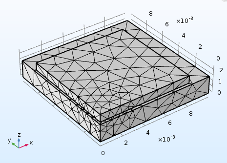
4. III. Experimental Procedure a) Finite Element Method (FEM)
The finite element method (FEM) is the dominant discretization technique in structural mechanics. To deal with a large problem, it subdivides a large problem into smaller, simpler parts that are called finite elements. The simple equations are used to model these finite elements and they are then assembled into a larger system of equations that models the entire problem.
5. b) Geometry Model
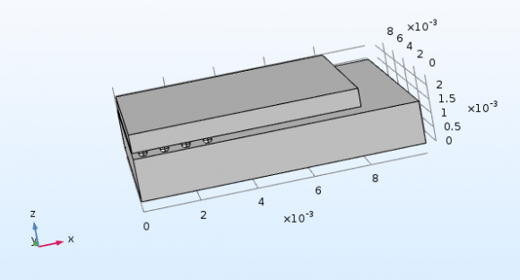
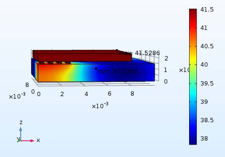
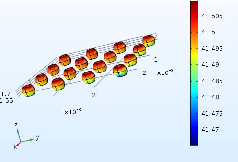
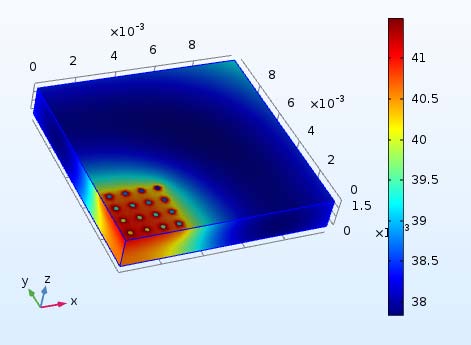
A typical 3-D model BGA structure with 16 solder joints with the diameter 0.3 mm are placed on the substrate and connect the electronic chip & one-quarter model is imported into simulation software COMSOL Multiphysics 5.2a to reduce the calculating time. Figure 1 shows the model, In figure 4, it is seen that among all the sixteen ball grids, the ball grid farthest away from the center has the maximum temperature at the top surface and the minimum one at the bottom surface. So, this temperature difference makes it easier to produce defects like fatigue and cracks.
Each other & pre-stress between them was ignored. The following table 2 shows the material parameters.
The environment temperature is 25 °Cand the power of the chip is 0.2 Watt. The convective heat coefficient between the chip and substrate is 10W/(m^2.k) [14]. The thermal stress analysis is conducted on the base of the thermal results obtained above.
6. IV. Simulation & Result Analysis a) Temperature Field
Figure 3 shows the temperature distribution of BGA model. It indicates that the maximum temperature temperature is on the substrate. The heat generated by the chip transfers to the substrate via the solder joints. Also, the heat also dissipates to the surrounding environment. Finally, a steady state is found.
is on the surface of the chip and the minimum Figure 5 shows the temperature distribution of the substrate, From figure 6, the maximum stress happens on the outside corner of the ball joints because of heat dissipation. From Figure 7, the solder joints have the highest stress value due to the higher thermal expansion coefficient than the substrate & the chip and the maximum & highest displacement of the solder joints happens in the same place with the maximum stress [14].
The maximum value of temperature and thermal stress are 41 degree Celsius & 199MPa respectively.
7. V. Factors Influencing Thermal Stress
Maximum stress plays a significant role in affecting the reliability and efficiency of BGA packaging. Various factors were considered for optimization. In future work, by using these different factors, a standard BGA model can be designed where maximum stress can be lowered and also can be more reliable and efficient.
8. a) Influence of Ball Pitch
| Component | Size (mm) |
| Chip | 8×8×0.65 |
| Ball Grid | 0.3 |
| Substrate | 10×10×1.5 |
| Component | Chip | Ball grid | Substrate |
| Material | Si | Sn-Pb | Epoxy |
| Thermal Conductivity (W/m.K) | 120 | 30 | 0.2 |
| CTE | 2.6 | 24.5 | 18 |
| Poisson's ratio | 0.28 | 0.35 | 0.38 |
| Stress (MPa) | ||||||||||
| Max. | ||||||||||
| 55 | 0.65 | 0.75 | 0.85 | 0.95 | 1.05 | |||||
| Ball Pitch (mm) | ||||||||||
| Max. Stress (MPa) | 170 180 190 200 210 | 179 0.55 | 190 0.65 | 194 0.75 Chip Thickness (mm) 197 0.85 | 203 0.95 | 1.05 | XVIII Issue III Version I | |||
| Max. Stress (MPa) | 0 50 100 150 200 250 | 145 8 | 170 9 | 190 10 Substrate Width (mm) 197 11 | 201 12 | 13 | Journal of Researches in Engineering ( ) Volume | |||
| Max. Stress (MPa) | 0 50 100 150 200 250 | 205 0.22 | 198 0.27 | 190 Ball Diameter (mm) 156 0.32 | 145 0.37 | 0.42 | Global | |||
| © 2018 Global Journals | ||||||||||