1.
Introduction odern wireless communication system requires simple structure, lightweight, low profile, and high gain antennas to assure high efficiency, mobility, and reliability characteristics. Microstrip antenna satisfies such requirements. This antenna provides all of the advantages of printed circuit technology. These features of Microstrip antennas create them public in many wireless communication applications such as radar, satellite communication, medical applications, etc. [1]. The restrictions of Microstrip antennas are narrow frequency band and disability to operate at high power levels of a coaxial line, waveguide or even strip line.
Therefore, the defy in Microstrip antenna design is to increase the bandwidth and gain [2]. Different array configurations of Microstrip antenna can give high gain, wide bandwidth and improved efficiency. The distribution of voltages through the elements of an array depends on feeding network. Suitable feeding network cumulate all of the induced voltages to feed into one point [3]. The proper impedance matching over the series and corporate feeding array configurations supplies high efficiency Microstrip antenna. Power distribution through antenna elements can be modified by corporate feed network. The corporate feed network can lead beam by introducing phase change [2].
In the array antennas, elements can be fed by a single line or by several lines in a feed network configuration. Based on their feeding methods, arrays are classified as Series feed network and T-shaped corporate feed network. Series-feed Microstrip array is molded by intersecting all the elements with high impedance transmission line and feeding the power at the first element. Because the feed arrangement is compact the line losses related to this type of array are lower than those of the corporate-feed type [2]. Seriesfed arrays can be conveniently fabricated using photolithography for both the radiating elements and the feed network. However, this technique is limited to arrays with a fixed beam or those which are scanned by varying the frequency, but it can be applied to linear and planar arrays with single or dual polarization. Also, any changes in one of the elements or feed lines affect the performance of the others. Therefore in a design, it is important to be able to take in to account these and other effects, such as mutual coupling, and internal reflections. Those who have been designing and experiment arrays antennas mention that radiation from the feed line, using either series or corporate-feed network, is an earnest problem that limits the crosspolarization and sidelobe level of the arrays. Both cross polarization and sidelobe levels can be improved by isolating the feed network from the radiating face of the array. This can be accomplished using either probe feeds or aperture coupling. The main limitation in seriesfeed arrays is the big variation of the impedance and beam-pointing direction over a band of frequencies [2]. M II.
2. Arrays And Feed Networks
Performance of antenna arrays depends on our ability to feed the array elements with input currents having accurate phase relationships. This can be accomplished by using appropriately designed "feed networks" consisting of transmission line (TL) segments. We continue our study of antenna arrays with examples illustrating feed network design issues. The Microstrip antenna can be agitated either by a Microstrip line or coaxial probe. It can also be excited indirectly using electromagnetic coupling or aperture coupling and a coplanar waveguide feed, in which case there is no direct metallic contact between the feed line and the patch [4]. Feeding technique effective the input impedance and characteristics of an antenna and is an influential parameter. Elements of an array can be fed by a single line, known as a series-feed network, or by multiple lines, known as a corporate-feed network, shown in Fig 1. III.
3. Corporate Feed Network
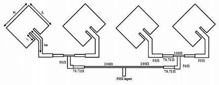
This Network gives more control of the feed of each element (amplitude and phase) and they are perfect for multi-beam arrays or formed-beam arrays. The amplitude can be changed with an amplifier or an attenuator when the phase can be controlled using a phase shifter. This network is used to supply power division of 2n (i.e. n = 2, 4, 6, etc.). This idea can be checked by using either tapered lines as shown in Transformers.
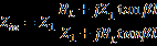
This power split can be achieved by using three port power dividers of equal division (3dB) with the use of a T-junction power divider. An ideal power divider is lossless, reciprocal and matched at all ports. A Tjunction power divider is reciprocal and can be considered lossless if the transmission line loss is not taken into account [5]. Helmholtz reciprocity theorem (generalized by Carson) states that "If an emf (electromagnetic force) is applied to the terminals of an antenna A and the current measured at the terminals of another antenna B, then an equal current (in both amplitude and phase) will be obtained at the terminals The following formula is applicable when the transformer is a quarter-wavelength or an odd multiple of a quarter-wavelength for a perfect impedance match:
A quarter-wave transformer with the input impedance of ZC = 50? and load impedance of ZL = 100 ? is equal to Z0 = 70.71?. These formulas explain the values used in Fig 3 . IV.
4. Beeds In Transmission Lines
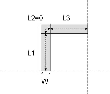
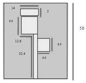
There is no best way to bend a Microstrip or stripline transmission line. The first problem is that the discontinuity changes the line characteristic impedance; without compensation, the bend adds shunt capacitance. But in reality, the small capacitance that is usually a result doesn't change the circuit's performance very much. The other problem associated with bends it can cause far more damage to the intended performance of a highly tuned circuit: the effective length of the transmission line becomes shorter than the centerline length. Show Fig 6. V.
5. Quarter-Wave Transform
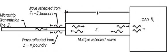
In the case of mismatch in impedance between two points on a transmission line can be compensated with a (?/4) quarter-wave transformer [7]. The quarterwave transformer (?/4) is a very profitable matching technique that also explains the properties of standing waves on a mismatched line. First, an impedancebased illustration of how a quarter-wave transformer works will be qualified; then a more intuitive illustration that is similar to ruinous interference in thin films will be discussed. In a quarter-wave transformer, a load resistance RL needs to be matched to the characteristic feed line impedance Z0 through a short length of transmission line of unknown length l and impedance. The input impedance Z1 looking into the matching section of line is given by: In the case of an ideal transition with no reflections at the interface between Microstrip Zin = Z0 and load, and this gives us characteristic impedance Z 1 as: which is the geometric mean of the load and source impedances. From this conFig, there will be no standing waves on the feedline although there will be standing waves on the quarter wave transformers (?/2) matching section. In fact, any odd multiple (2n + 1) of l= ?/4 will also work.
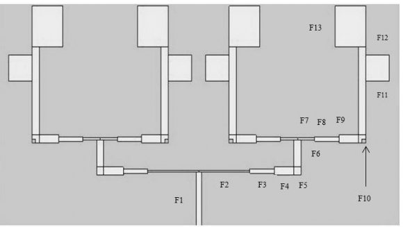
When the line length is precisely ?/4 the reflected wave from the load destructively interferes with the wave reflected from Z0, Z1 the interface and they cancel each other out. It should be noted that this method can only match a real load. If the load has an appreciable imaginary component, it must be matched differently. It can be transformed into a purely real load, at a single frequency, by adding an appropriate length of feedline. Fig 8 shows the complete feed network with the patches. There are many transmission lines, V grooves, power splitters, and quarter wave transformers.
6. Gain Measurements
To gain measurements, we use the friis formula.
By writing the Friis formula as (dB), we obtained:
Where FSL is Free Space Loss. Pr, and Pt are received and transmitted power respectively. Gr and Gt are received and transmitted Gain respectively. D, the distance between transmitter and receiver, ? is Wavelength. From the measuring the transmitted and received power
7. Conclusion
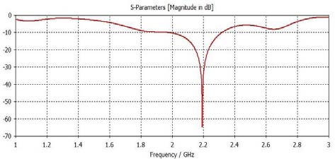
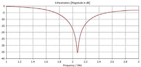
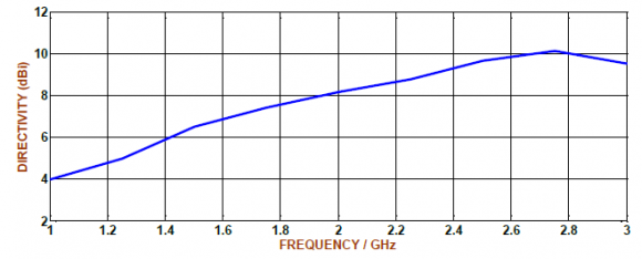
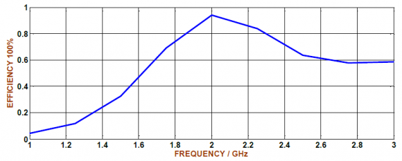
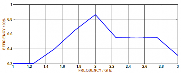
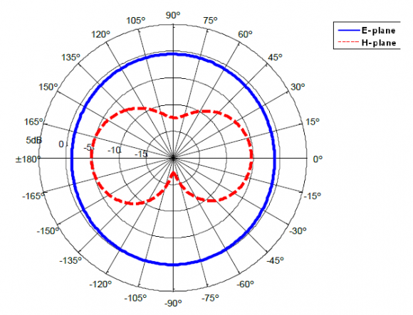
In this research, single and four elements Microstrip patch antenna array by corporate (parallel)feed network at 2.1 GHz application are presented. This suggested array antenna is investigated and successfully simulated in this research; the simulated return loss, radiation pattern and bandwidth showed well performance for the single antenna at 2.1GHz. They investigate higher directivity, gain and better bandwidth with practical technology and theoretical analysis. The results of the array antenna are compared with those of single antenna of novel patch Microstrip antenna. It is found that there is an important change in the radiation features of array antenna. It can be concluded from the top results that, designing a proper feed network and impedance matching are very important parameters in Microstrip patch antenna design (single and array). Selection a proper position for ending the feed line affects the overall performance of the antenna. The simulation results show return loss of -64.45 dB for the array antenna and -36.44 dB for the single antenna.
From the results, it is seen that the suggested array and single antenna achieve good value of directivity, gain performance and the antenna has good bandwidth, this makes the suggested antenna design suitable for use in the 2.1GHz applications as a transmitting and a receiving.
![Fig 2 or by using (?/4) quarter wavelength transformers as shown in Fig 3 [2].](https://engineeringresearch.org/index.php/GJRE/article/download/1749/version/100931/5-Design-and-Manufacturing_html/20377/image-3.png)


![of antenna A if the same emf is applied to the terminals of antenna B [6]". A T-junction can be modeled as a junction of three transmission lines as shown in Fig 4.](https://engineeringresearch.org/index.php/GJRE/article/download/1749/version/100931/5-Design-and-Manufacturing_html/20380/image-6.png)


| Simulated | Measuring | |
| Antenna | gain | gain |
| (dB) | (dB) | |
| Single | ||
| Microstrip | 2.206 | 2.04 |
| Antenna | ||
| Array | ||
| Microstrip | 8.506 | 8.313 |
| Antenna |