1. Introduction
arbon Nanotubes are sheets of graphite rolled in the shape of a tube. Depending on chirality they can be either metallic or semiconducting. Carbon Nanotubes were discovered by Iijima at the NEC Fundamental Research Laboratory while he used a high resolution transmission electron microscope (TEM) to observe byproducts of carbon which had been generated by an arc between two carbon electrodes (Iijima, 1991). After that momentous development has been achieved by understanding the characteristics and searching possible applications of these on semiconductor technology. They have high elastic modulus, small weight and are predicted to be the strongest fibers. Carbon Nanotube's strength and flexibility are their unique properties. The fascinating electronic properties of them depend drastically on both the diameter and the chirality of the hexagonal carbon lattice along the tube (Mintmire et al., 1992;Hamada et al., 1992;Saito et al., 1992). Because of its excellent conductivity and high dielectric properties, CNTs play a vital role in different nano electronic devices such as transistors, digital logic devices, memory components, etc (Heinze et al., 2002).
The fundamental strategy for improving the performance of VLSIs is scaling down of electronic devices. According to the ITRS the gate length of MOSFETs will be less than 16 nm in 2016 (ITRS, 2003). If this continues then the MOSFETs will reach its limiting size very soon. Thus the semiconductor industry is searching for different materials to integrate with the current silicon-based technology and in the long run, possibly replace it if required. In this regard the carbon nanotube field effect transistor (CNTFET) will be the most promising alternatives for its unique properties. It was demonstrated long before in 1998 (Tans et al., 1998). Carbon nanotube field-effect transistors offer high mobility for ballistic transport, high mechanical and thermal stability with high resistance to electro migration, attracting strong interest as alternative high device technologies for the future nano electronics applications (Avouris et al., 2007). Recently, a carbon nanotube transistor, which integrates ultra-short channel, thin high-k top gate insulator and excellent Pd source-drain contact is demonstrated using a self-align technique (Javey et al., 2008).
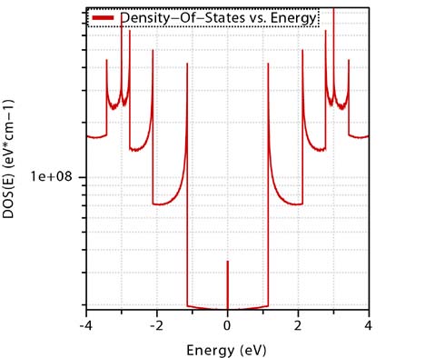
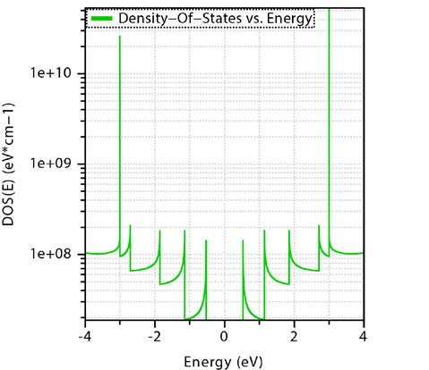
This paper proposes CNTFET with ZrO 2 as gate oxide which is also one of the most promising devices. This paper has been devised into main two sections. In the first section, the mobility of CNTs has been discussed with analyzing the Density of State (DOS) of different types of nanotubes and in the second part, the proposed CNTFET device modeling has been described with its parameters, along with simulation results.
2. II.
3. Carbon Nanotube
Carbon is an element with symbol C. Its atomic number is 6 (1s 2 2s 2 2p 2 ). Carbon is a group 14 element that resides above silicon on the periodic table. It is nonmetallic and tetravalent making four electrons available to form covalent chemical bonds. Carbon has four electrons in its valance shell like silicon (1s 2 2s 2 2p 6 3s 2 3p 2 ) and germanium (1s 2 2s 2 2p 6 3s 2 3p 6 3d 10 4s 2 4p 2 ). There are several allotropes of carbon like graphite, diamond and amorphous carbon (Carbon materials research group, University of Kentucky). When carbon atoms are arranged in crystalline structures composed of benzene like rings, they form several allotropes that contain totally exceptional electronic properties.
The physical properties of carbon vary widely with the allotropic form (List of thermal conductivities, Wikipedia). Diamond, carbon nanotubes and graphene have the highest thermal conductivity of all known materials (e.g., diamond: 900-2300 Wm ?1 K ?1 , carbon nanotube: 3180-3500 Wm ?1 K ?1 ) (Faisal and Ali, 2015) under normal conditions.
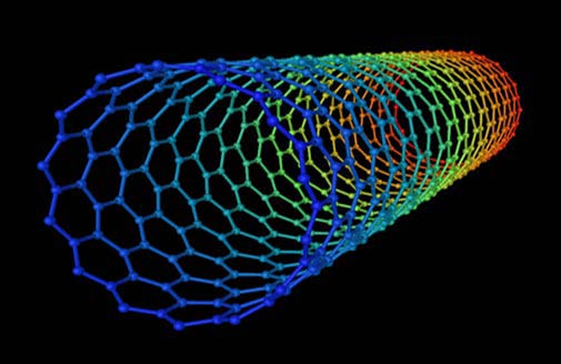
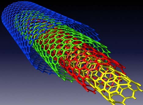
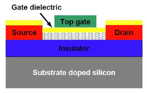
Carbon Nanotubes (CNTs) are an allotrope of carbon. Carbon nanotubes have many forms, differing in length, thickness and in the type of helicity and number of layers. It can be categorized into Single Walled Carbon Nanotube (SWCNT) and Multi Walled Carbon Nanotube (MWCNT) shown in Fig. 1 and 2. The carbon nanotubes have diameters from less than 1nm to 50 nm. These possess excellent mechanical and transport properties too.
The rolled graphene (CNT) can be explained by a coordinate of indices (n, m), which is known as Chiral Vector. It represents whether CNT is metallic or semiconducting and diameter of CNT. The table shown below describes "Chirality of carbon nanotube. The diameter of carbon nanotube is given by: IV.
4. Modelling of Cntfet
The proposed device is formed with a (10, 0) CNT. So the channel diameter =0.782885nm. For gate insulation ZrO 2 (k = 25) is used. Energy gap for a nanotube is given by:
2 c-c a? Eg = channel diameter(2)Where: ? = The nearest neighbor-hopping parameter (? = 2.5-3.2) Using ? = 3, the energy gap is 1.0882eV. The parameters used in proposed model and calculations are given in Table 3. Conductance between two leads source and drain is defined in terms of current and voltage: I = GV. Using Landauer formula (Nazarov and Blanter, 2009), conductance is expressed by the following equations:
5. Global
where, q is the charge of electron and h is the Planck's constant. T is known as the transmission function in terms of energy that represents the probability of an electron injected at one end of a conductor will emit at the other end. T can be expressed as:
r a S 0 D 0 T = trace T G Î?" G ? ? ? ?(4)G 0 r G 0 a represents the retarded and advanced Green's function of the nanotube and Ð?" D , Ð?" S are the coupling of the CNT to the source and the drain. The retarded Green's function is calculated by: ( )
-1 r 0 S D G = EI - ? --? ? (5)where, E is Fermi energy, I is the identity matrix, H is the Hamiltonian of the nanotube. ?S, ?D is the self-energy terms at the source and drain coupling of the contacts are the calculated using the broadening function of the self-energy terms at the source and drain. The nanotube behaves as the conducting channel in the CNTFET from the source to drain; it depends on the current density of the tube. The current density is a measure of the density of flow of an electric current per unit area across a section. The current density is an area density described by J. The current through an area A is simply the flux of the current density through that area as shown below: ? I = J.dA (6) Using the charge density within the device, the NEGF transport equation is solved teratively with the posison equation until self-consistant potential distribution is found. Finally the current is calculated using the Landauer Böuttiker expression:
( ) ( ) ( ) s d d 4d T E f E -f E dE I = h ? ? ? ? ?(7)T is the transmission probability across the source/drain; f S and f D are the source/drain Fermi-Dirac distribution functions consistent potential; The equation is solved simultaneously to evaluate and characterize the performance of these devices.
V.
6. Simulations
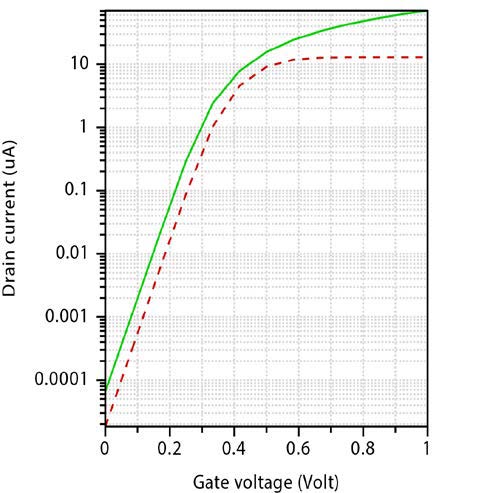
Hafnia (HfO 2 ) adopts the same structure as zirconia (ZrO 2 , K=~25). Unlike TiO 2 (k = 40), which features six-coordinate Titanium in all phases, zirconia and HfO 2 consists of seven-coordinate metal centers (Miikkulainen et al., 2013;Faisal and Ali, 2012). Hafnium-based oxides were introduced by Intel in 2007 as a replacement for silicon oxide as a gate insulator in field-effect transistors (Source: INTEL). We simulate the I-V Characteristics of CNTFET using ZrO 2 as gate insulator for proposed model. The high-K gate insulator and bigger CNT diameter allows higher drain current.
Figure 7 shows the output characteristics of the proposed CNTFET. The channel allows the current to flow when the gate voltage is greater than 0.3 V. So the on current is 70 ?A at Vg = 2.0 V and Vd = 1.0 V and the off current is 6.61e-05 ?A at Vg = 0V and Vd = 1.0 V.
7. Material
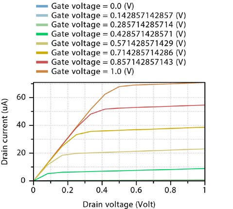
Young's modulus (GPa) Tensile strength (GPa) Electrical conductivity (mho/m) In order to achieve a relatively large transconductance the CNT must have large channel diameter. The larger the transconductance, the greater the gain it will deliver. As the diameter gets smaller this reduces the carrier mobility, changing the transconductance. The transconductance behavior is obtained at 0.78 nm diameter, with different drain voltage (Fig. 8). The transconductance varies by a factor of 10/V depending on the amount of voltage applied to the gate. However, the increase of VG will reduce the allowed voltage signal through the drain. Quantum capacitance is associated with the properties of channel material. As the density of state is finite in a semiconductor quantum well, the Fermi level needs to move up above the conduction band edge as the charge in the quantum well increases. This movement of Fermi level requires energy and this conceptually corresponds to quantum capacitance. Figure 9 shows the quantum capacitance versus the gate voltage at different drain voltages. It is clear that a higher quantum capacitance can be found at a gate voltage 0.42 or 0.57 volt (for proposed model).
8. Fig. 11: Mobile charge behavior at drain voltage
As insulator thickness approaches the nanometer range, the insulator capacitance becomes comparable to the inversion layer capacitance, which means that the QC and the centroid capacitance start to affect the gate capacitance.
Figure 10 shows the mobile charge behavior as a function of gate voltage. It is noticed that increasing the drain voltage beyond a specific value has no longer an effect on the shape of the curves since the mobile charge remains constant. It is also observed that low drain voltage produces higher mobile charge and high drain voltage produces lower mobile charge. Also, it has been noticed that the mobile charge increases with the reduction in gate insulator thickness. Figure 11 shows the mobile charge behavior as a function of drain voltage.
9. VI.
10. Conclusion
The proposed parameters and gate dielectric of CNTFET make the transistor a challenge to develop and control the aspects of it such maximum transconductance. We found two regions for maximum transconductance. Zirconia is used in optical coatings and in DRAM capacitors as a high-k dielectric and in advanced metal-oxide semiconductor devices. The advantage for proposed CNTFET is its high dielectric constant: The dielectric constant of ZrO 2 is 4-6 times higher than that of SiO 2 . In recent years, zirconium oxide (as well as doped and oxygen-deficient zirconium oxide) attracts additional interest as a possible candidate for resistive-switching memories (Lin, 2011).
VII.
| Performance Analysis of Enhanced Carbon Nanotube Field Effect Transistor (CNTFET) using Zirconia as |
| Gate Dielectric |
| Year 2017 |
| 52 |
| II Version I |
| Journal of Researches in Engineering ( ) Volume XVII Issue F |
| Energy gap | 1.0882 eV | Gate oxide thickness | 1.6 nm |
| CNT diameter | 0.78 nm | Gate dielectric (ZrO2) | 25 |