1.
Introduction he waves at an interface between an isotropic medium and a uniaxial crystal characterized by its effective permittivities have been first demonstrated in [1]. The existence of these surface waves in some material examples is studied in [2], discussing the challenge posed by their experimental observation. The novelty and potential importance of Dyakonov waves for integrated optics applications were described in a stream of papers [3][4][5].
In near-infrared and visible wavelengths, the behavior of nanolayered metal-dielectric (MD) compounds is similar to plasmonic crystals. In this case a simplified description of the medium by using the long-wavelength approximation can be justified; the homogenization of the structured metamaterial can also be employed [6][7][8]. It is interesting to note that the second-rank tensor representing the medium permittivity includes elements of opposite signs, thus yielding extremely anisotropic metamaterials under certain conditions [9,10]. This category of nanostructured media opens the wide avenues for the practical applications from biosensing to fluorescence engineering [11].
The existence of surface waves when dealing with anisotropic media possessing the indefinite permittivity was reported for the first time in [12]. This study was dedicated mainly to surface waves enabling sub-diffraction imaging in magnifying superlenses [13], where the surface waves exist at an interface between a metal and an all-dielectric birefringent metamaterial. Dealing with hyperbolic media, however, the authors concluded only with an indefinable analysis of surface waves.
In this paper we retake the task and perform a thorough analysis of surface waves traveling in infinite MD lattices. Our approach is to use the effectivemedium approximation.
The investigated structure is shown in Fig. 1. It should be mentioned that an infinite periodic model consisting of alternating layers of a metal and a conventional dielectric is placed on the left of the homogeneous dielectric. The effective dielectric tensor components parallel ( || ? ) and perpendicular ( ? ? ) to the anisotropy axis are described in [14] as:
d m d d m m d d d ? d ? ? + + = ? (1) d m d d m m d d ? d ? d ? + + = / / 1 || (2)2. Geometry of the Problem
3. Plasmonic lattice
Metal/dielectric/ Semiconductor dielectric metal valid in the long-wavelength limit. However, the field varies significantly on the scale of one period due the excitation of surface plasmon (SP) polaritons at metal/dielectric interfaces. Therefore, the approximation in Eqs. ( 1) and ( 2) may not be applicable in some spectral ranges.
4. III. Numerical Analysis of Dispersion Characteristics
Herein we discuss the numerical solution to the dispersion relation [15], either obtained for metamaterial/air interface or for metamaterial/metal and metamaterial/semiconductor interfaces.
5. a) Metamaterial/Air interface
The dispersion relation [15] is graphically represented in Fig. 2 for the MD crystal displayed in Fig. 1 at x < 0, considering different widths of the dielectric d d and assuming, that we are dealing with metamaterial/air interface. Fig. 2 shows the dispersion of surface waves at a metamaterial/air interface. The case (d d > 0) corresponds to classic surface waves well known for conductive interfaces [16]. Thus, this example illustrates the verification of our methodology [15]. In addition, the light line in vacuum is plotted in Fig. 2 as dashed line. Our calculated data corresponds to the data of [17] where also a complete discussion of the surface wave characteristics in this case can be found.
As can be seen from Fig. 2, the frequency range for surface waves can be controlled by the fill factors of the air and metal sheets in the MD compound.
If we decrease the thickness of the dielectric d d , the dispersion curve moves to a lower frequency. The dependence of the frequency range for the surface wave existence on the thickness of the dielectric layer provides additional degree of freedom to control surface waves.
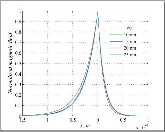
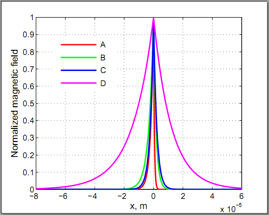
Fig. 3 shows the profiles of the magnetic field along the x axis for the investigated case, i. e. metamaterial/air. The magnetic field has been obtained when ? = 4?10 6 1/m. The wave field is tightly confined near x = 0 for all the thicknesses of the dielectric d d .
The conducted analysis shows, that the frequency range for the surface wave existence seems to be narrow. Thus, we shall leave the geometry unchanged but assume that instead of an interface between a metamaterial and air we will be dealing with an interface between a metamaterial and a metal. Doing so, we can extend the frequency range for the surface wave existence. It should be noticed, that each medium is capable of supporting propagating surface waves separately.
6. b) Metamaterial/Metal interface
The dispersion curves for the matamterial/metal structure are presented in Fig. 4. The calculations were performed using the following parameters for bulk silver: ? p = 2297.09 THz, ? ? = 5.2 [18]. As in previous cases we discuss the effects of the thickness of the dielectric d d on the dispersion curve. It should be noticed that the upper and the lower limits move to lower frequencies when d d is decreased. However the lower limit moves faster than the upper one. The mentioned issue leads to a broader frequency range for the surface wave existence. It should be mentioned, that the wave field is tightly confined near x = 0 for all the thicknesses of the dielectric d d . It is interesting to note that in the case of a metamaterial/air interface (Fig. 3) the tighter confinement near the boundary x = 0 is exhibited in the metamaterial while in the case of a metamaterial/metal interface the tighter confinement is in the metal.
7. c) Metamaterial/Semiconductor interface
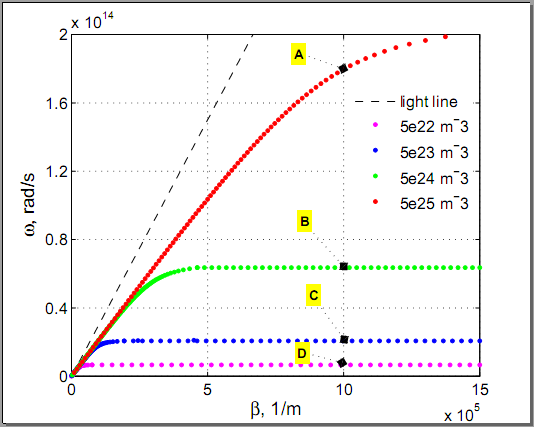
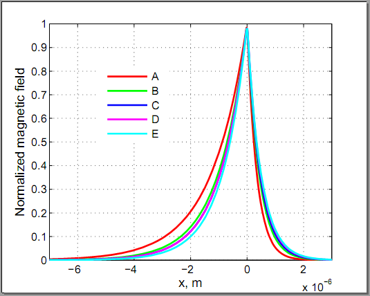
It is interesting to notice, that he case of heavy doped Si is considered, assuming that the doping level is N 1 =5?10 19 cm -3 [19]. An average effective mass m 1 for electrons is 0.26m 0 with m 0 being the free-electron mass, and ? ?1 = 11.68. To date it is well known, that the presence of semiconductor in the structure can tune the properties of the investigated system in the easy way. Thus in Fig. 7 we present the dispersion curves of the surface wave dealing with the different concentrations of the Si. Fig. 8 shows the profile of the magnetic field along the x axis for the investigated case, i. e. metamaterial/semiconductor. Fig. 8 shows the magnetic field for the points when ? = 1.5?10 6 1/m. The tight confinement of the wave field is observable near x = 0 for all the thicknesses of the dielectric d d . It is interesting to note that the tighter confinement near the boundary x = 0 is exhibited in the semiconductor.
Moreover, it is of particular interest to plot the profile of the magnetic field along the x axis, when the doping level of the silicon changes. The results are depicted in Fig. 9 being d It is interesting to notice, that the lowest confinement in this case is produced for the lowest doping concentration of silicon.
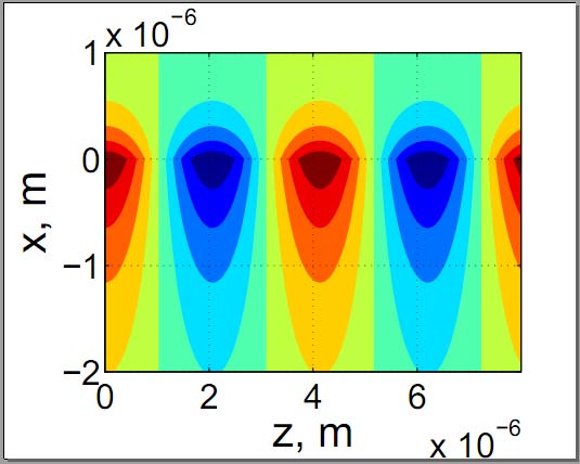
It is valuable to confirm the presence of SP waves for all the investigated cases. In the insets of Figs. 2, 4 and 6 we show the nature of the magnetic fields for all the investigated cases.
IV.
8. Conclusions
The surface waves at the boundary of hyperbolic metamaterial have been studied for three different cases: metamaterial/ air, metamaterial/metal, metamaterial/semiconductor. The dependences of the longitudinal propagation constant on the propagation frequency have been examined. It is established that one can tune the frequency range of surface waves by varying the thickness of dielectric sheets. It is also revealed that this frequency range can be broadened by three different manipulations:
? decreasing the thickness of the dielectric in the metal-dielectric compound; ? dealing with the metamaterial/metal structure;
? increasing the doping concentration of the semiconductor, if considering the metamaterial/semiconductor interface.