1. I. Introduction
he increased use of non-linear loads deteriorate power system voltage and current waveforms as they inject harmonics into the system. This results in increased losses, lower efficiency, failure of equipment etc. in the power system. Apart from voltage and current harmonics, voltage sag, voltage swell, voltage outage also can lead to poor quality of power [1]. Harmonic compensation and voltage regulation have become more important as imbalance in the voltage and presence of harmonics have been serious issues. Hence, there is a great need to mitigate these power quality issues.
The introduction of advanced power electronics technology has led to the development of active power filters which are viable solution to these power quality problems [1,2].
The general arrangement of Unified power quality conditioner is shown in Fig. 1. The main function of a UPQC is to compensate voltage and current harmonics.
The UPQC combines series and shunt active filters with a common dc link. The series active filter suppresses voltage distortions while the shunt filter Author ?: e-mail: [email protected] cancels current distortions such that this combination allows simultaneous compensation of voltages and currents supplied to the sensitive load to see that they are sinusoidal and balanced. Fig. 1 : General configuration of UPQC Multilevel inverters play an important role in the reduction of harmonic content in the voltages and currents. The multilevel inverters can synthesize high output voltage from smaller voltage levels and thus the current ripples and voltage harmonics are reduced. The UPQC presented in this work consists of three level converter topology [3,4]. The performance of UPQC can be optimized because of reduction in the size of passive components and transformers [4].
2. II. The Upqc Controller
The UPQC controller is composed of PLL circuit, Reference Voltage Algorithm and Reference Current Algorithm [4,5,6].
The PLL circuit has the system voltages Vab and Vcb i.e (Vab =Vas -Vbs, Vcb = Vcs -Vbs) as inputs and the outputs are the signals Pll_a, Pll_b and Pll_c as shown in Fig. 2.
3. Fig. 2 : The synchronizing ciruit
The PLL circuit guarantees the load voltages and source currents to be balanced sinusoidal waveforms at fundamental frequency.
The reference current control strategy is shown in Fig. 3. The reference currents algorithm control block determines six reference currents (i aref1, i bref1, i cref1 ) and (i aref2 ,i bref2 ,i cref2 ) by using the outputs of PLL (Pll-a,Pll-b,Pllc) , the DC link voltages (V dc1 ,V dc2 ) and the load currents (I al, I bl ,I cl ) as inputs. The shunt active power filter will then synthesize the reference currents. The "reference voltage algorithm" shown in Fig. 4 calculates, the reference voltages (V aref , V bref , V cref ) by using system input voltages (V as , V bs , V cs ) and PLL outputs(pll-a, pll-b, pll-c) that will be synthesized by the series power converter.
4. III. Switching Strategy of Three Level Converters
In order to illustrate the switching control technique applied to the series and shunt active power converters, a basic three level NPC (Neutral Point Clamped ) topology as shown in Fig. 5 is used [7,8].
5. Fig. 5 : Three level Neutral point clamped converter
Each leg has four switching devices connected in series. As an example, phase "a" is considered to explain the behavior of the circuit.
The output of the inverter can take three voltage levels based on the switching states of the devices. The output Va is positive when switches S1a and S2a are ON, it is negative when S3a and S4a are turned ON, and it is '0' when switches S2a and S3a are ON. The switching states of the devices and the corresponding output voltages with respect to the dc mid-point are indicated in the following Table I.
The switching strategy of the series active filter is shown in Fig 6 . In this technique, the reference signal is compared with measured signal, the error is amplified and processed by PWM generator to obtain Va_PWM. This signal is compared with two triangular waves of different limits having unit magnitude. The switching control strategy of the shunt active converter is shown in In this work, Phase Disposition multicarrier scheme is applied to Sinusoidal PWM. In this modulation, the reference sine wave is compared with the level shifted carrier triangular waves for producing the pulses. For a three level inverter, two triangular carrier waves of same frequency and amplitude are compared with the reference wave. The plane is divided into 6 triangular major sectors numbered I to VI each of 60 0 of fundamental cycle. There are 4 minor sectors within each major sector such that 24 minor sectors are there in the plane.
The vertices of these minor sectors represent the voltage vectors. In the above plane, V0 is the zero voltage vector, large voltage vectors are represented by V13, V14, V15, V16, V17, V18 and V7, V8, V9, V10, V11, V12 are the medium voltage vectors. To determine the location of the command vector V* in a given major sector, first space vector phase angle' ?' is calculated and then sector is determined. The determination of major sector is done as follows:
Table I : Determination of major sector
6. Range of '? '
Major sector number
0 ? ? < 60 0 I 60 ? ? < 120 0 II 120 ? ? < 180 0 III 180 ? ? < 240 0 IV 240 ? ? < 300 0 V 300 ? ? < 360 0 VILet us consider space vector diagram of sector I as shown in Fig . 9. It contains 4 minor triangles D1, D7, D13 and D14. The reference vector can be located in any of these 4 regions, where each region is limited by three adjacent vectors.
If the triangular sector where the command vector lies is defined by vectors Vx, Vy, and Vz assuming their durations Tx, Ty, and Tz respectively and Tx + Ty + Tz = Ts ,then V*= Vref can be synthesized by Vx, Vy, and Vz as follows : (?/6<?<?/3), V* lies in sector D14 and can be synthesized by Vectors V2. V7, and V14. X, Y, and Z can be determined as follows:
X = 2m [cos (?) - ?????? ? ?3 ] Y = -1 + m 4 ?????? ? ?3 Z = 2-2m [cos (?) + ?????? ? ?3 ]Similar argument can be applied ,when the reference vector lies in the others major sectors. The above calculations for the entire coordinate plane can be obtained by replacing ? by ? -60 0 , ? -120 0 , ? -180 0 , ? -240 0 , and ? -300 0 respectively.
7. V.
8. Simulation Results
Simulations were carried out in MATLAB/ SIMULINK on three-level Neutral Point Clamped Unified Power Quality Conditioner connected to a non-linear load employing Sinusoidal Pulse Width Modulation and Space Vector Pulse Width Modulation techniques and the results are presented below. FFT analysis is carried out in order to measure %THD in the load voltage and source current.
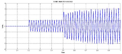
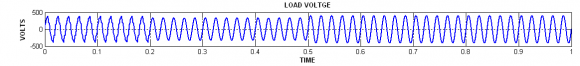
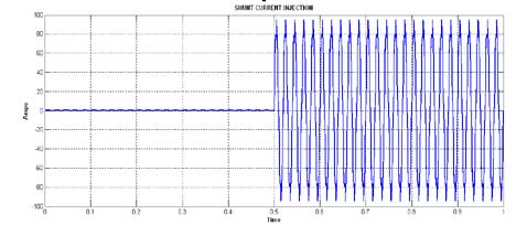
To study the performance of the UPQC, 5 th and 7 th harmonics are deliberately injected into the system and simulations were carried out to show the response of the UPQC. The series inverter is put into operation at 0.2sec and shunt inverter at 0.5sec.FFT analysis is carried out on the load voltage at 0.1sec and the THD is found to be 12.32%. In the second analysis, FFT is done at 0.8sec i.e. after connecting UPQC and THD is reduced to 2.01% FFT analysis of source current FFT analysis of source current before connecting UPQC FFT analysis of source current after connecting UPQC FFT analysis is carried out on the source current at 0.1sec before connecting UPQC and the THD is found to be 33.97%. In the second analysis, FFT is done at 0.6sec after connecting UPQC and THD is 2.01% b) Simulation results of 3level UPQC with SVPWM 19, it is clear that the harmonics are reduced to some extent after 0.1 sec where series filter is switched ON and from 0.25sec onwards there is a considerable reduction in the harmonics as both filters are in operation.
9. FFT analysis of load voltage
FFT analysis of load voltage before connecting UPQC FFT analysis of load voltage after connecting UPQC FFT analysis is carried out on the load voltage at 0.05sec before switching ON series and shunt inverters and the THD is found to be 12.32%. FFT analysis of load voltage again carried out at 0.3sec after connecting both series and shunt filters and THD is found to be 1.27%.


![b) Space Vector Pulse Width Modulation ii Space Vector diagram of 3-level SVPWM inverterThe space vector diagram of 3-level inverter is shown in Fig.8[9,0,11].](https://engineeringresearch.org/index.php/GJRE/article/download/1399/version/100700/2-Simulation-and-Analysis-of-Power_html/15224/image-6.png)
| SWITCHING STATES | OUTPUT | |||
| VOLTAGE | ||||
| S1a | S2a | S3a | S4a | Va |
| ON | ON | OFF | OFF | +Vdc/2 |
| OFF | OFF | ON | ON | -Vdc/2 |
| OFF | ON | ON | OFF | 0 |