1. I. Introduction
any different PWM methods are available to achieve these aims: wide linear modulation range, reduced switching loss, lesser total harmonic distortion in the spectrum of switching waveform, easy implementation, less memory space and computation time on implementing digital processors. The most widely used PWM schemes for Multi-level inverters are the carrier based PWM (sinetriangle PWM or SPWM) and space vector based PWM. These modulation techniques have been studied extensively and compared for the performance parameters for two level inverters [1,2].
The SPWM techniques are more flexible and simple to implement, but the maximum peak of the fundamental component in the output voltage is limited to 50% of the DC link voltage and the extension of the SPWM techniques into over-modulation range is difficult [2].
The SVPWM technique presented for multi-level inverters can also work in the over-modulation range. The SVPWM technique gives more fundamental voltage and better harmonic performance compared with SPWM technique [3][4][5].The maximum peak of the fundamental component in the output voltage obtained with space vector pulse width modulation is 15% more than with the sine-triangle modulation technique [2,3]. But the conventional space vector PWM technique requires sector identification and look-up tables to determine the timings for various switching vectors of the inverter in all the sectors [3,4].This makes the implementation of the SVPWM technique is complicated.
Based on the arrangement of carrier waves, the PWM techniques can be classified as Phase Disposition (PD), Phase Opposition Disposition (POD), Alterative Phase Opposition Disposition (APOD), Phase Shifted Carrier PWM (PSCPWM). PD, POD and APOD are level shifted carrier PWM methods whereas; PSCPWM is the phase shifted carrier method.
This paper focuses on different control strategies and suitable modulation strategy is selected based on the outputs obtained through the simulations for cascaded multi-level inverters.
2. a) Phase Disposition (PD)
This technique requires (m-1) carrier waveforms for an m-level phase waveform. All the carriers are in same phase and level shifted equally. The Fig. 1 shows the arrangement of carriers for eleven level cascaded multilevel inverter. The ten carrier signals with same phase but level shifted equally are compared with reference signal.
3. b) Phase Opposition Disposition (POD)
This technique requires (m-1) carrier waveforms for an m-level phase waveform. Half of the carrier waveforms above and below are in phase, but there is 1800 phase shift between the above and below half as shown in Fig. 2. The significant harmonics are located around the carrier frequency fc for both the phase and line voltage waveforms.
4. Fig.2 : c) Alterative Phase Opposition Disposition (APOD)
This technique requires (m-1) carrier waveforms for an m-level phase waveform. The carriers are phase displaced each other by 1800 alternatively as shown in Fig. 3. The most significant harmonics are centered as sidebands around the carrier frequency fc and therefore no harmonics occur at fc. In this technique all the carriers are phase shifted by an angle 3600/N (where N is number of single phase inverter cells used in a phase leg). This strategy leads to the cancellation of all carrier and associated sideband harmonics up to 2Nth carrier group [6]. Fig. 4 shows the arrangement of carriers for an eleven level cascaded multilevel inverter.
For APOD, the first set of sideband harmonics is centered about the carrier frequency, while for PSCPWM the first set of sideband harmonics is centered about the 2Nth multiple of carrier frequency, where N is the number of h-bridges in each cascaded inverter phase leg. [7]. The total number of switch transitions for PSCPWM is exactly 2N times the number of switch transitions for APOD.
5. II. Modified svpwm
The conventional SVPWM for multilevel inverters involves mapping of the outer sectors to an inner sub hexagon sector, to determine the switching time duration, for various inverter vectors. Then the switching inverter vectors corresponding to the actual sector are switched, for the time durations calculated from the mapped inner sectors. It is obvious that such a scheme, in multilevel inverters will be very complex, as large number of sectors and inverter vectors are involved. This will also considerably increase the computation time for real time implementation.
A carrier based PWM scheme has been presented [8], where sinusoidal references are added with a proper offset voltage before being compared with carriers, to achieve the performance of a SVPWM. The offset voltage computation is based on a modulus function depending on the DC link voltage, number of levels and the phase voltage amplitudes.
A modulation scheme is presented where a common mode voltage of suitable magnitude is added to the reference phase voltage throughout the duration [4,5]. A modulation technique is presented in [7], where a fixed common mode voltage is added to the reference phase voltage throughout the modulation range. It has shown [9] that this common mode addition will not result in a SVPWM like performance, as it will not centre the middle inverter vectors in a sampling interval. The common mode voltage to be added in the reference phase voltages, to achieve SVPWM like performance is a function of the modulation index for multilevel inverters [9]. A simplified method, to determine the correct offset times for centering the time durations of the middle inverter vectors, in a sampling interval is presented [10]. To obtain the maximum possible peak amplitude of the fundamental phase voltage in linear modulation, the procedure for this is given in [11][12][13]
* a s a dc V T T V = (1) * b s b dc V T T V = (2) * c s c dc V T T V = (3) a T , bT and c T are the imaginary switching time periods proportional to the instantaneous values of the reference phase voltages This proposed SVPWM signal generation does not involve region identification, sector identification or look up tables for switching vector determination required in the conventional multilevel SVPWM technique. This scheme is computationally efficient when compared to conventional multilevel SVPWM scheme.
0 min [ ] 2 offset T T T = ? (4) 0 [ ] s effect T T T = ?(5)6. III. Simulation Results and Comparison
To Induction
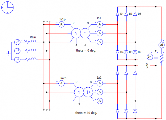
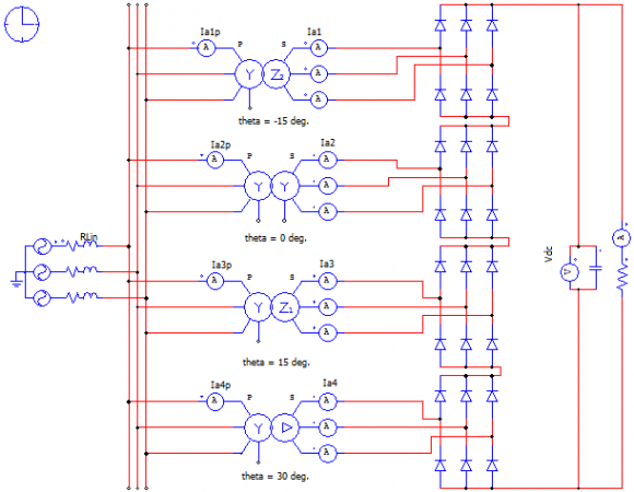
Fig. 6 : Cascaded 11 level Multilevel Inverter.
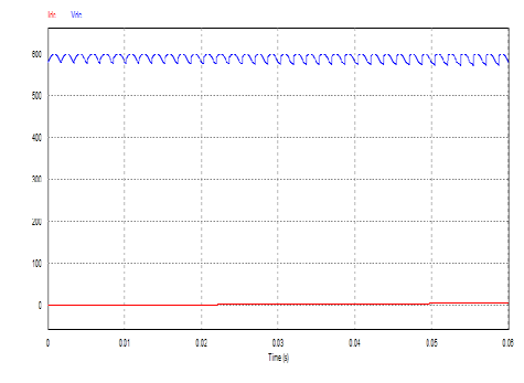
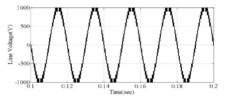
An eleven level cascaded multilevel inverter fed with Induction motor shown in Fig. 6 and for RL load is simulated. The carrier frequency fc is 1 kHz. The modulating pulses are generated by the comparing the reference wave with the triangular waves. For m level cascaded multilevel inverter m-1 carrier waves required.
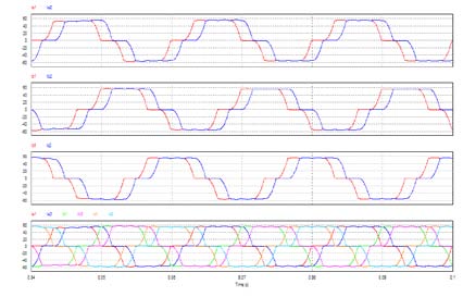
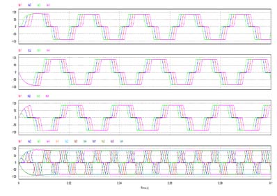
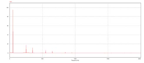
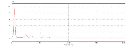
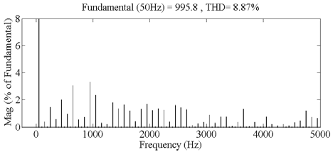
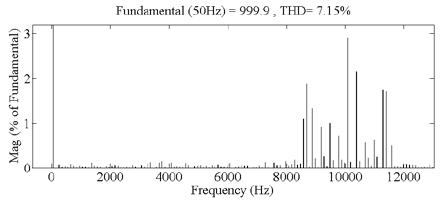
It is simulated for different carrier modulating techniques PDPWM, PODPWM, APODPWM and PSCPWM. Fig. 7 shows the generation of PWM pulses for Eleven Level Cascaded Multilevel Inverter by using PDSVPWM. Fig. 8 shows the generation of PWM pulses for Eleven Level Cascaded Multilevel Inverter by using PODSVPWM. Fig. 9 shows the generation of PWM pulses for Eleven Level Cascaded Multilevel Inverter by using APODSVPWM and Fig. 10 shows the generation of PWM pulses for Eleven Level Cascaded Multilevel Inverter by using PSCSVPWM. Here reference wave is generated by modified SVPWM technique. Fig. 11 shows the harmonic spectrum of line voltage for PSCSPWM. Fig. 12 shows the harmonic spectrum of line voltage for PDSPWM. Fig. 13 shows the harmonic spectrum of line voltage for PODSPWM and Fig. 14 shows the harmonic spectrum of line voltage for APODSPWM. It is observed that PDSPWM technique produces fewer harmonic with respect to other techniques. Fig. 15 shows harmonic spectrum of line voltage for an eleven level Cascaded Multilevel Inverter by using PDSVPWM technique. Fig. 16 shows harmonic spectrum of line voltage for an eleven level Cascaded Multilevel Inverter by using PODSVPWM technique. Fig. 17 shows harmonic spectrum of line voltage for an eleven level Cascaded Multilevel Inverter by using APODSVPWM technique and Fig. 18 shows harmonic spectrum of line voltage for an eleven level Cascaded Multilevel Inverter by using PSCSVPWM technique.
From Fig. 16, it is observed that the significant harmonics are located around the carrier frequency fc for the line voltage waveform in PODSVPWM.
From Fig. 17, it is observed that the most significant harmonics are centered as sidebands around the carrier frequency fc and therefore no harmonics occur at fc for APODSVPWM.
From Fig. 18, it is observed that the PSCPWM strategy leads to the cancellation of all carrier and associated sideband harmonics up to 2Nth carrier group.
For APOD and POD , no harmonic exists at pulse number P due to odd symmetry of their PWM wave forms. For PD, the wave forms is asymmetric and the harmonic at P is relatively high only for single phase, but for three phase the triplen harmonics of voltage will be eliminated, thus harmonics at P is eliminated if P is chosen as a multiple of three. So PD is more convenient due to very little values of other harmonics.
It is observed that the total harmonic distortion is less in PDSVPWM technique with comparison to other SVPWM techniques and all other SPWM techniques. Table 1 shows the Line voltage harmonic comparison of an eleven level cascaded multilevel inverter connected to RL and Induction motor loads for all the PWM techniques. It is observed from the table that PDSVPWM technique generates fewer harmonic with respect to all other methods.
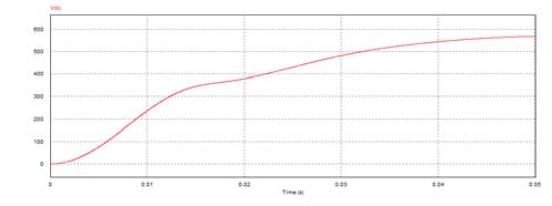
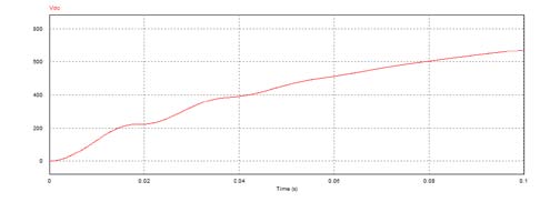
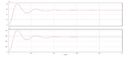
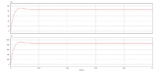
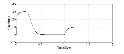
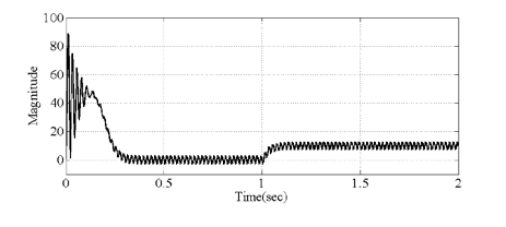
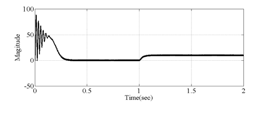
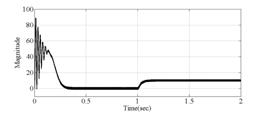
In this simulation the induction motor used is shows Induction Motor torque waveform for the Space Vector PWM technique PODSVPWM and Fig. 27 shows Induction Motor torque waveform for the Space Vector PWM technique APODSVPWM. Here the load torque is varied from 0 to 10 at 1 sec. It is observed that the motor torque reaches to steady state quickly by using various modified SVPWM techniques. involve region identification, sector identification or look up tables for switching vector determination required in conventional SVPWM technique. Simulation studies have been carried out on Cascaded multilevel inverter fed Induction motor and RL load for different PWM techniques. It is observed that Modified SVPWM technique has given better torque and speed performance of the motor, and it is also noticed that one of the modified SVPWM techniques is PDSVPWM technique which produces less harmonic distortion with respect to all other PWM techniques.
V. Acknowledgment


| S.No Type of PWM | % THD | Magnitude | ||
| of | ||||
| Fundamental | ||||
| I. | SPWM With RL Load | |||
| 1 | PDSPWM | 6.79 | 865.7 | |
| 2 | APODSPWM | 8.57 | 864.7 | |
| 3 | PODSPWM | 9.36 | 860.7 | |
| 4 | PSCSPWM | 10.81 | 692.5 | |
| II. | Modified SVPWM with RL load | |||
| 1 | PDSVPWM | 5.51 | 999.4 | |
| 2 | PSCSVPWM | 7.31 | 998.6 | |
| 3 | APODSVPWM | 8.51 | 1005 | |
| 4 | PODSVPWM | 8.85 | 996.4 | |
| III. SPWM With IM load | ||||
| 1 | PDSPWM | 6.76 | 865.2 | |
| 2 | PSCSPWM | 1083 | 693 | |
| 3 | APODSPWM | 8.46 | 868.6 | |
| 4 | PODSPWM | 9.99 | 869.8 | |
| IV. Modified SVPWM with IM load | ||||
| 1 | PDSVPWM | 5.24 | 1000 | |
| 2 | PSCSVPWM | 7.15 | 999.9 | |
| 3 | APODSVPWM | 8.87 | 995.8 | |
| 4 | PODSVPWM | 8.80 | 996.7 | |