1. Introduction
n order to achieve the high speed and low power demand in DSP applications Braun's multiplier are broadly used. The Braun's multiplier is generally called as the Carry Save Array Multiplier. The architecture of a Braun's multiplier consists of AND gates and full adders. The prolific growth in semiconductor device industry has been Indicates to the high performance portable systems with enhanced reliability in data transmission. In order to maintain the high performance fidelity applications, emphasis will be on incorporation of low power modules in future system design [1][2][3][4][5]. The design of such modules power consumption or dissipation in fundamental arithmetic computation units such as adders and multipliers. This implies a need to design low power multipliers towards the development of efficient power & high-performance systems. The selection of the most efficient implemented multiplication has continually challenge DSP system designers [6][7]. Every system designer offers a wide range of tradeoffs in terms of speed, complexity and power consumption. Input sequences to the multiplier can be fed in parallel, serial or a hybrid (parallel serial) this proposal approaches gives high processing speed. Usually Parallel multipliers are adopted at the expense of high area complexity.
2. Multiple
parallel multiplications Algorithms (architectures) [8] have been proposed to reduce the chip area increase the speed of the multipliers' and reduce the power dissipation using various techniques. Several of these techniques reduce the power dissipation by eliminating spurious transitions in the circuit [9,11]. The architecture is simulated with the cadence micro wind software. As shown in the above Table .1. The proposed work of the MOS transistors with normal threshold voltage was used at critical path. It is observed that 4-bit Braun multiplier using proposed Work4 Power Delay Product 119 femito (10 -15 ), with Reference paper [11], it is observed that 46% of power Delay Product has been reduced.
3. II.
4. Proposed Work
As shown in the above Table .2. The proposed work of the MOS transistors with low threshold voltage was used at critical path. It is observed that 4-bit Braun multiplier using proposed Work2 we got Power Delay Product 111 femito (10 -15 ), but comparatively to the Reference paper [11], it is 51% of power Delay Product has been reduced.
As shown in the above Table .3. The proposed work of the MOS transistors with high threshold voltage was used at critical path. It is observed that 4-bit Braun multiplier using proposed Work1 Power Delay Product 120 femito (10 -15 ), with Reference paper [11], it is observed that 47% of power Delay Product has been reduced.
As shown in the above Table
5. Conclusion
The present paper demonstrated the improvement in parameters v/s, Area, power, and delay with reduction in number of transistors to implement Full adder circuits. The simulations were performed using 90nm Micro wind 3 CMOS layout CAD Tool In this paper power consumption & Power Delay Product is calculated the results are optimized power consumption of 46% and Power Delay Product is 56 % still the performance of 4-Bit CMOS Braun Multiplier is improved by incorporating techniques which support reduced transistor implementations.
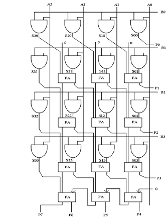
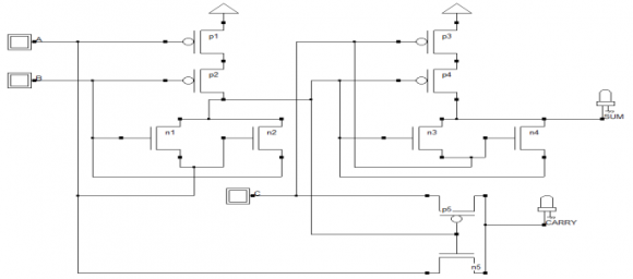
![full adder has been designed with 10 MOS Transistors for the implementation of logic expression of Eq. (1) & Eq. (2). The 1-bit full adder circuit consists of three modules, XNOR-I, XNOR-II, and MUX. The XNOR-I and XNOR-II modules are designed using 4 MOS transistors considering two inputs and one output, and MUX module is designed with two MOS transistors for optimum operation. The implementations of full adders are shown in Fig .1to Fig.4the XNOR and XOR logic is combined with 6 MOS transistors and MUX logic with 2 MOS transistors for optimum operation. The implementation of full adder with 10 MOS transistors is shown in Fig.5Full Adders propose were is presented in the reference paper[10]](https://engineeringresearch.org/index.php/GJRE/article/download/1223/version/101357/4-Design-of-Low-Power_html/29068/image-2.png)
| 4-bit Multiplier | 60.055 | 4.270 | 256 | 5534 | |
| proposed | |||||
| work2 | |||||
| 4-bit Multiplier | 25.594 | 4.695 | 120 | 5516 | |
| proposed | |||||
| work3 | |||||
| 4-bit Multiplier | 74.600 | 6.860 | 511 | 5660 | |
| proposed | |||||
| work4 | |||||
| 4-bit Multiplier | 24.524 | 6.025 | 147 | 5752 | |
| proposed | |||||
| work5 | |||||
| Proposed 4-bit Braun Multiplier Low V T (Low Threshold voltage) & High V T (High Threshold voltage) Table.4 Power(µw) Delay(ns) Power Delay Product Area (µm 2 ) | |||||
| Multipliers Proposed | Power(µw) | delay(ns) | femito(10 -15 ) Power Delay | Area (µm 2 ) | |
| Proposed 4x4 Multipliers 2011 IEEE paper 4-bit Multiplier proposed work1 4-bit Multiplier proposed work2 2011 IEEE 4-bit Reference Multipliers paper 4-bit Multiplier proposed work1 4-bit Multiplier proposed work2 4-bit Multiplier proposed 2011 IEEE paper 4-bit Multiplier proposed work1 4-bit Multiplier proposed work2 4-bit Multiplier work3 4-bit Multiplier proposed work4 4-bit Multiplier proposed work5 work5 proposed work3 4-bit Multiplier proposed work4 proposed 4-bit Multiplier | Power(µw) 45.686 30.702 25.992 45.686 54.302 30.089 28.404 45.686 24.448 26.743 64.600 25.063 27.444 28.321 29.235 | delay(ns) 5.270 4.691 4.277 5.270 4.695 4.615 4.695 5.270 4.270 4.695 6.435 4.785 4.990 5.340 4.695 | Power Delay Product femito(10 -15 ) 237 144 111 237 Product femito (10 -15 ) 254 138 133 237 104 125 415 119 136 151 137 | Area (µm 2 ) 5610 5354 5654 5610 5712 5456 5910 5610 5524 5918 5706 5661 5700 5959 5736 | Issue IX Version I of Researches in Engineering ( ) F Volume XIV |
| 4-bit Multiplier proposed work3 4-bit Multiplier proposed work4 4-bit Multiplier proposed work5 | 26.194 28.475 29.586 | 4.690 4.785 5.055 | 122 136 149 | 5504 5500 57.26 | Global Journal |
| Braun Multiplier High V T (High Threshold voltage) Table.3 | |||||
| Proposed | Power(µw) | delay(ns) | Power Delay | Area (µm 2 ) | |
| 4-bit Multipliers | Product femito(10 -15 ) | ||||
| 2011 IEEE | 45.686 | 5.270 | 237 | 5610 | |
| paper | |||||
| 4-bit Multiplier | 26.553 | 4.695 | 124 | 5530 | |
| proposed | |||||
| work1 | |||||